Advanced Technologies
Introduction
Over the course of 18 years in the Functional Verification field, I’ve been asked many times what it is that we actually do. Are our desks draped in wires, cables, and measurement devices? Are we testers? What exactly are we testing? What is verification?
In a world dominated by software and applications, comparatively little attention is given to the hardware that allows software and applications to run. So let’s take a look at what’s involved in manufacturing that small, arcane square that we sometimes see if we look inside our PC or laptop – a chip:

A chip is usually called an Integrated Circuit (IC), which falls into two main categories: digital and analog. Digital ICs are generally called ASICs (Application Specific Integrated Circuits) because they are designed to implement a specific function. They may look minuscule, but a regular ASIC can hold billions of transistors, making the fabrication process very complex and expensive.
The digital IC design process is usually divided into three main stages:
- System-level design: at this stage the architects define what the chip will be doing.
- RTL design: the required behavior is translated into RTL (Register Transfer Level) – this is still just code, and the chip doesn’t actually exist yet.
- Physical design: the RTL code is transformed into the actual design; this is the first prototype, and usually there will be a few more coming.
The first step is specifying what the chip should do; the second one is how the chip will implement that functionality, and the last step does not influence the chip’s functionality but will define how fast it operates, and how much it will cost.
Chip Design flow
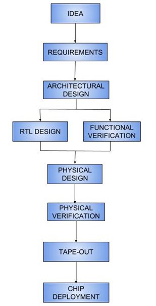
The process of creating a chip is briefly illustrated in the picture below:

The process begins with an idea, often derived from market trends and customer needs. People always want a faster switch, a thinner laptop, or a GPU that can process high-definition images. This idea is refined until the requirements emerge from the process.
Based on these requirements, the architecture team defines how the chip will operate, what will be the principal data flows going through it, and its fundamental configurations. The architects also define at this stage the clock frequencies the chip will operate at and will estimate the chip’s power consumption and size. All these aspects are part of the architecture specification.
The next step is to define the micro-architecture specification (MAS). Micro-architecture defines the implementation methods for the architecture and establishes the major components of the chip, along with the interfaces between them.
Once the micro-architecture specification is decided, two important steps follow in parallel: RTL design and design verification. At this stage, the designers use Hardware Description Languages (HDLs) such as Verilog and VHDL to implement the micro-architecture’s specification requirements. Design verification is the process of verifying that the RTL design works according to the specification, using dedicated languages such as Specman or SystemVerilog, known as Hardware Verification Languages (HVLS).
The next step is physical design and verification: the RTL is only a behavioral model of the actual functionality of the chip, so during this step, a set of libraries of available logic gates are used to map the RTL to actual electronic components such as transistors, resistors, and capacitors.
This phase concludes with a design reaching tape-out: the chip is manufactured and sent back to the lab for post-silicon validation, where a team of engineers runs different test vectors on it. At this stage debugging is difficult, since there is little information about the chip’s internal states and signals. Any real issue found at this point has to be sent back to the RTL team for fixing and then to the design verification team for subsequent validation. After this eventuality, all the above steps will need to be performed again.
This is one reason why it’s important that the design verification phase take place at the right time in the project flow. It’s much easier and cheaper to fix bugs at the design stage than when the chip is already being manufactured — not to mention the inevitable loss of credibility when a bug is identified in a production chip.
Chip design flow is similar to the process of building a house: we don’t start by digging the foundation and building the walls, because we don’t yet have all the information we need, which risks the integrity of the structure. We also don’t yet know the cost and the time needed for building.
Therefore the architect researches first what kind of house is needed, before building the plans, validating them with structural and installation engineers, and estimating the cost and duration of the project.
Design Verification
Once the micro-architecture specification is defined, RTL design and design verification start in parallel, using the micro-architecture specification as the reference. The reasons for having a separate team for the verification are:
- To avoid making the same assumptions as the design team, since this may cause bugs to remain undiscovered.
- To save development time by allowing the design and verification teams to work in parallel.
One might ask why the Functional Verification role is not taken on by the designers that implement the module, who are well acquainted with its functionality. In fact, this approach has worked in the past, when design complexity was lower; but today’s designs are much more complex, with a huge number of states. In order to make sure that all the required scenarios are generated abstractly, high-level programming languages (HVL) must be used. These languages use OOP principles to allow the development of robust, scalable, and reusable code. On top of that, they also make use of constrained random generation in order to produce meaningful scenarios for the verification process.
Due to the high complexity of the design, and the huge number of internal states and input combinations, several verification techniques are employed at different stages of the project:
- Formal verification attempts to check that the design requirements are met, using formal methods of mathematics.
- Functional verification (simulation) verifies that the design works according to the specification.
- Emulation uses FPGA (Field Programmable Gate Array)-based machines to load the Verilog code and to simulate the hardware. This approach has fewer debug capabilities but has the advantage of being much faster than simulation.
Functional Verification Flow
Though no two projects are alike, and each project comes with its own challenges and features, there are some major steps that are prerequisites for a successful verification project:
- The first is to understand the design functionality by reading the specification and also consulting with the architect. The golden rule here is not to presume the hardware’s behavior based on the designer’s understanding of the specifications, since this is likely to obscure bugs in the chip’s practical functionality.
- Next is the creation of the verification plan: this is a document with several sections detailing which features and scenarios should be checked (test plan section), how they will be checked (checker’s plan section), and the metrics to show that they were checked (coverage plan section).
- After the plan is reviewed and approved, the verification engineers begin implementing the verification environment using one of the HVLs mentioned above. This process requires programming skills using basic OOP features and usually takes the majority of the time allocated for Functional Verification.
- Implementing tests and coverage from the verification plan: a test is a set of configurations that will instruct the verification environment to generate a specific scenario. Some tests may be pre-figured, but in general random tests are preferred, since there is a higher chance they will hit previously hidden weaknesses in the design.
- Running regressions: a regression means that all the existing tests are run multiple times so they can cover as many scenarios and states as possible. Every failure is analyzed and debugged by the verification engineer, together with the designer, and the outcome could reveal either a bug in the verification environment or a bug in the design.
- Sign off: this is one of the trickiest stages of the project since the verification engineer must decide if the verification is actually concluded. The honest answer is that it never really is since it’s almost impossible to know if all the design’s internal states and transitions were hit. However, the risk of closing the verification without finding all the bugs can be minimized using indicative metrics:
- The chip demonstrates 100% functional coverage.
- All tests produce zero failures over several weeks.
- No critical bugs were found in the final few weeks.
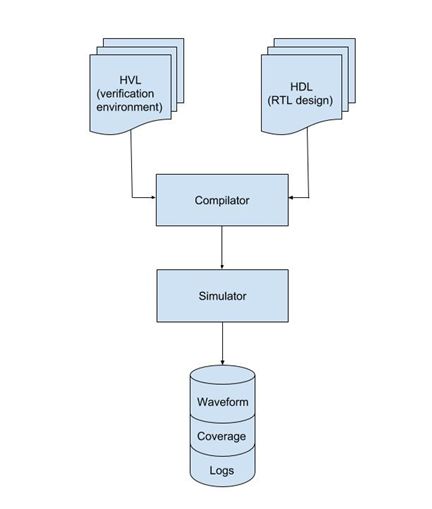
Once the verification environment code is stable enough, one of the main activities is ‘running tests/simulations. The verification environment code is compiled together with the RTL code, using special tools. The result is then ‘simulated’, meaning that the design receives stimuli from the verification environment and processes this according to the specification. The simulation will produce waveforms, logs, and coverage results that will be analyzed by the verification engineer in order to understand the simulation result (passed, design bug, environment bug).

ASIC Functional Verification is a very demanding and challenging pursuit, but it’s also very rewarding. Engineers working in this field are always up to date with the latest developments in the industry. They gain knowledge about digital circuits and various protocols and standards used in the semiconductor industry. Another important area is object-oriented programming and algorithms, since implementing the verification environment is essentially a programmer’s job. Even though it’s a little bit ‘behind the scenes, this aspect brings significant contributions to the design architecture and functionality of the chip, because these are, in effect, the product’s first users. Being a successful verification engineer requires a lot of creativity and lateral thinking, along with a logical and analytical mind.